Materials
Characterization Lab.-II
Laboratory report on
Four-point Prob
Experiment
Submitted by
Shibu Meher
17MM01019
Semester VII
 _
_
School of Minerals, Metallurgical and Materials Engineering
Indian Institute of Technology, Bhubaneswar, India
Date of Submission: 01/09/2020
Four-point Prob Experiment:
Objectives
To determine the relationship between temperature and resistivity of germanium and to estimate the band gap energy using four-point prob method.
Introduction
Four-point prob method is used to measure the resistivity of a semiconductor material. Figure 1 shows the setup of four-point prob method [1].
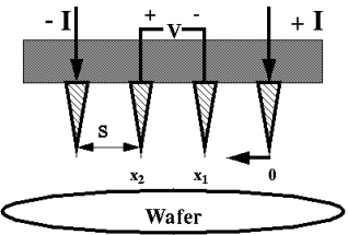
Figure 1. Four-point Prob Method Schematic
The probes are made up of tungsten with sharp tip on one end and the other end is attached with a string to avoid damage of the sample during probing. The spring is attached to an auto mechanical stage. The outer two probes are connected with a high impedance current source and the inner two probes are connected to a voltmeter.
If the constant current from one outer probe to the other is I, then the current flowing from one inner probe to the other will be I. So, the voltage measured between the two inner probe is given by
![]()
Now the resistivity is given by
![]()
After including a correction factor the
effective resistivity is given by
Where the correction factor is given by
![]()
Where S is the separation of two
consecutive probe and W is the thickness of the sample.
The relation between effective
resistivity and the temperature is given as follows.
![]()
where ![]() is the band gap of the material, k is the
Boltzmann constant and K is a constant which depends on temperature and
mobility of charge carriers.
is the band gap of the material, k is the
Boltzmann constant and K is a constant which depends on temperature and
mobility of charge carriers.
So, the slop of the line fit of plot ![]() will give the
value of
will give the
value of ![]() .
Then multiplying the slope with 2k will give the value of bandgap.
.
Then multiplying the slope with 2k will give the value of bandgap.
Experiment details
Apparatus Required
1. Probes arrangement
2. Ge crystal sample
3. Oven
4. Multirange digital voltmeter
5. Constant current generator
6. Oven power supply
Precautions Required
1. The probes should be placed at the centre of the crystal plate.
2. It should be ensured that the four probes are touching the crystal by checking the electrical conductivity.
3. Proper pressure should be applied to ensure the sample is not damaged by the probe and to ensure the electrical path is complete. Too much pressure can damage the sample. Very little pressure may result in probe not touching the sample.
Procedure
1. The sample was placed on the base plate and the four probes were pressed gently at the centre of the sample and electrical contact was ensured.
2. Outer probes pair was connected to a constant current source and the inner pair was connected to the terminal of the voltmeter with polarity as shown in Figure 1.
3. The sample and prob arrangement were placed inside the oven.
4. Current was set to 8 mA and the voltage across the inner probe was measured for different temperatures. The observation has been shown in Table 1.
Results
Given information
S = 2 mm, W = 0.66
mm, so ![]() 4.200892
4.200892
I = 8 mA, so ![]() (Calculated
in Table 1).
(Calculated
in Table 1).
Now, ![]() has been
calculated in Table 1.
has been
calculated in Table 1.
Values of ![]() have been
calculated for different value of temperature in Table 1.
have been
calculated for different value of temperature in Table 1.
Figure 2 shows
the plot of ![]() . The slope (m) of the plot is 3570 and we know the
value of Boltzmann constant (k) to be
. The slope (m) of the plot is 3570 and we know the
value of Boltzmann constant (k) to be ![]() . So, the
value of band is estimated as follows.
. So, the
value of band is estimated as follows.
![]()
Table 1. Calculation
of ![]()
|
Sl.
No. |
Temperature
T (K) |
Voltage
in V |
|
|
|
|
|
1 |
310 |
0.524 |
0.8230973 |
0.195933929 |
0.003226 |
-1.62998 |
|
2 |
320 |
0.415 |
0.6518805 |
0.15517668 |
0.003125 |
-1.86319 |
|
3 |
330 |
0.355 |
0.5576327 |
0.132741498 |
0.00303 |
-2.01935 |
|
4 |
340 |
0.316 |
0.4963716 |
0.118158629 |
0.002941 |
-2.13573 |
|
5 |
350 |
0.217 |
0.3408628 |
0.081140577 |
0.002857 |
-2.51157 |
|
6 |
360 |
0.146 |
0.2293363 |
0.054592278 |
0.002778 |
-2.90786 |
|
7 |
370 |
0.11 |
0.1727876 |
0.041131168 |
0.002703 |
-3.19099 |
|
8 |
380 |
0.085 |
0.1335177 |
0.031783175 |
0.002632 |
-3.44882 |
|
9 |
390 |
0.065 |
0.1021018 |
0.024304781 |
0.002564 |
-3.71708 |
|
10 |
400 |
0.05 |
0.0785398 |
0.018695986 |
0.0025 |
-3.97945 |
|
11 |
410 |
0.039 |
0.0612611 |
0.014582869 |
0.002439 |
-4.22791 |
|
12 |
420 |
0.031 |
0.0486947 |
0.011591511 |
0.002381 |
-4.45748 |
|
13 |
430 |
0.026 |
0.0408407 |
0.009721913 |
0.002326 |
-4.63337 |
|
14 |
440 |
0.021 |
0.0329867 |
0.007852314 |
0.002273 |
-4.84695 |
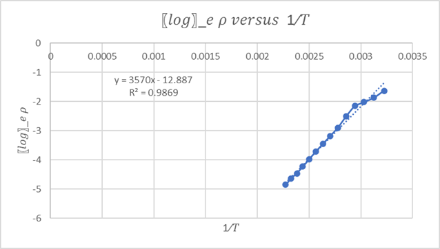
Figure 2. Plot of ![]()
Discussion
From the plot of ![]() it is clear
that resistivity decreases as temperature increases and vice versa. This can be
explained by the fact that increase of temperature increases the energy of atom
and hence the energy of valance electron, which enables more valence electron
to cross the band gap and to go to the conduction band. The more the number of
conduction electron higher is the conductivity and lower is the resistivity.
it is clear
that resistivity decreases as temperature increases and vice versa. This can be
explained by the fact that increase of temperature increases the energy of atom
and hence the energy of valance electron, which enables more valence electron
to cross the band gap and to go to the conduction band. The more the number of
conduction electron higher is the conductivity and lower is the resistivity.
The value of
bandgap is found to be ![]() (Standard Value is 0.7 eV). This means a valence electron needs to have this
much energy to cross the bandgap and become a conduction electron. This also
means that there is a potential difference of 0.615277 V from valence band to
conduction band. So, the valence electron needs to overcome the potential field
of strength 0.615277 V to become a conduction electron.
(Standard Value is 0.7 eV). This means a valence electron needs to have this
much energy to cross the bandgap and become a conduction electron. This also
means that there is a potential difference of 0.615277 V from valence band to
conduction band. So, the valence electron needs to overcome the potential field
of strength 0.615277 V to become a conduction electron.
Conclusion
In this experiment the resistivity of the intrinsic Ge crystal with respect to different temperature was found out using four-point probe method. Using the relationship between resistivity and temperature the bandgap of the material was estimated.
Suggestion for improvement of the experiment – The value obtained is close to the standard value of band gap. If a thicker crystal is used then the value may be closer to the standard value. This is because the effect of the nonconductive plate below the specimen will not be there.
References
[1] https://physics.iitm.ac.in/~ph5060/manuals/Fourprobe.pdf
[2] Introduction of Solid State Physics, by C. Kittel IVth edition.
[3] Fundamental of Semiconductor Devices by J. Lindmayer and C.Y. Wriegley
Answer to the
questions (if any):